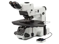
MX63 / MX63L
Semiconductor Wafer & Flat Panel Display Inspection Microscopes
Optimize Your Wafer Inspection Microscope and Workflow
Learn how semiconductor wafer manufacturers can improve wafer inspection quality control by optimizing their equipment and workflows.
Capabilities of Near-Infrared Imaging for Electronics and Semiconductor Inspection
Discover how Evident inspection microscopes enhance near-infrared imaging for semiconductor inspection.
Circuit Pattern Inspection on Wafer Samples
Discover how Evident’s MX63/MX63L industrial microscopes for semiconductor/FPD inspection provide an efficient alternative to conventional observation methods of wafer samples.
The Invisible Becomes Visible: MIX Observation and acquisition
MIX observation technology produces unique observation images by combining darkfield with another observation method, such as brightfield, fluorescence, or polarization. MIX observation enables users to view defects that are difficult to see with conventional microscopes. The circular LED illuminator used for darkfield observation has a directional darkfield function where only one quadrant is illuminated at a given time. This reduces a sample’s halation and is useful for visualizing a sample’s surface texture.
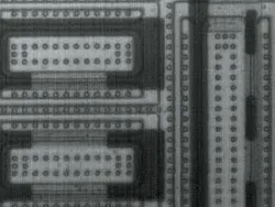
Structure on semiconductor wafer
Photoresist residue on a semiconductor wafer
User-FriendlyIntuitive Microscope Controls: Comfortable and Easy to Use
The microscope’s settings are simple to operate, making it easier for users to make adjustments and reproduce system settings.
Find the Focus Quickly: Focus Aid
Inserting a focus aid in the optical path allows easy and accurate focusing on low-contrast samples, such as bare wafers.
Combined high numerical aperture and long working distance
Objective lenses are crucial to a microscope’s performance. The new MXPLFLN objectives add depth to the MPLFLN series for epi-illumination imaging by maximizing numerical aperture and working distance at the same time. Higher resolutions at 20X and 50X magnifications typically mean shorter working distances, which forces the sample or objective to be retracted during objective exchange. In many cases, the MXPLFLN series’ 3 mm working distance eliminates this problem, enabling faster inspections with less chance of the objective hitting the sample.
Two Systems Accommodate Diverse Sample Sizes
The MX63 system can accommodate wafers up to 200 mm while the MX63L system can handle wafers up to 300 mm with the same small footprint as the MX63 system. The modular design makes it easy to customize the microscope for your specific requirements
IR compatibility
Infrared observation can be conducted with the IR objective lenses, which enable the operators to nondestructively inspect the inside of IC chips packed and mounted on a PCB, utilizing the characteristics of silicon that transmit infrared light. 5X to 100X IR objectives are available with chromatic aberration correction from visible light wavelengths through the near infrared. Especially with an objective lens of 20X or more, the aberration caused by the silicon layer covering the observation object can be corrected by the correction collar to obtain a clear image.
Software Industrial applications


